Magnetron Sputtering
Home » Magnetron Sputtering Deposition
Magnetron Sputtering

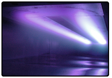
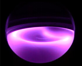
Magnetron Sputtering is a Plasma Vapor Deposition (PVD) process in which a plasma discharge is created by ionizing a process gas in a high vacuum environment. The positively charged ions from the plasma are attracted by an electrical field superimposed on the negatively charged electrode or “target”. The positive ions are accelerated by potentials ranging from a few hundred to a few thousand electron volts and strike the negative electrode with sufficient force to dislodge and eject atoms from the target through a momentum transfer process. These atoms will be ejected in a typical line-of-sight cosine distribution from the face of the target and will condense on all surfaces that are placed in proximity to the magnetron sputtering cathode.
Targets can be fabricated from almost any material that one subsequently wants to deposit on the surface of the component facing the electrode typically referred to as the “substrate”. The possibilities are very diverse, and you can sputter almost any material from conductive elemental metals, ceramics, glass, compounds and alloys. Conductive materials can be deposited using a direct current (DC) power supply and insulators can be deposited by using a radio frequency (RF) power supply. 13.56 MHz is one of the frequencies in the RF spectrum that has been allocated to “industrial applications” as is by far the most common frequency used in the sputtering application.

Magnetron sputtering deposition uses a closed magnetic field to trap electrons, enhancing both the efficiency of the initial ionization process and allowing a plasma to be generated at lower pressures which reduces both background gas incorporation in the growing film and energy loses in the sputtered atom through gas collisions. This technique was pioneered in the late 1800’s and gained commercial success in the Microelectronic and Architectural Glass industry in the 1960’s and 1970’s. At the present time, magnetron sputtering sources are commercially available in many geometric configurations where the targets can be circular, rectangular, or tubular in form. Novel approaches based on sweeping the magnetic field over the surface of the target have been engineered and deployed to drive application-specific solutions.
For more information on Magnetron Sputtering Deposition or to discuss your project, call +1-412-469-8466 or contact us online.
Magnetron Sputtering
Magnetron Sputtering is a Plasma Vapor Deposition (PVD) process in which a plasma discharge is created by ionizing a process gas in a high vacuum environment. The positively charged ions from the plasma are attracted by an electrical field superimposed on the negatively charged electrode or “target”. The positive ions are accelerated by potentials ranging from a few hundred to a few thousand electron volts and strike the negative electrode with sufficient force to dislodge and eject atoms from the target through a momentum transfer process. These atoms will be ejected in a typical line-of-sight cosine distribution from the face of the target and will condense on all surfaces that are placed in proximity to the magnetron sputtering cathode.
Targets can be fabricated from almost any material that one subsequently wants to deposit on the surface of the component facing the electrode typically referred to as the “substrate”. The possibilities are very diverse, and you can sputter almost any material from conductive elemental metals, ceramics, glass, compounds and alloys. Conductive materials can be deposited using a direct current (DC) power supply and insulators can be deposited by using a radio frequency (RF) power supply. 13.56 MHz is one of the frequencies in the RF spectrum that has been allocated to “industrial applications” as is by far the most common frequency used in the sputtering application.
Magnetron sputtering deposition uses a closed magnetic field to trap electrons, enhancing both the efficiency of the initial ionization process and allowing a plasma to be generated at lower pressures which reduces both background gas incorporation in the growing film and energy loses in the sputtered atom through gas collisions. This technique was pioneered in the late 1800’s and gained commercial success in the Microelectronic and Architectural Glass industry in the 1960’s and 1970’s. At the present time, magnetron sputtering sources are commercially available in many geometric configurations where the targets can be circular, rectangular, or tubular in form. Novel approaches based on sweeping the magnetic field over the surface of the target have been engineered and deployed to drive application-specific solutions.
For more information on Magnetron Sputtering Deposition or to discuss your project, call +1-412-469-8466 or contact us online.